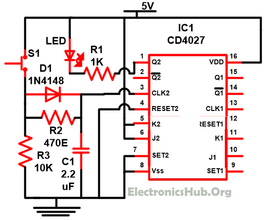
JK Flip Flop with CD4027 Circuit Diagram:
Circuit Components:
IC CD4027 Resistor R1(1K) R2(470E) R3(10K) C1(2.2uf) S1 LED D1(1N4148)
JK Flip Flop with CD4027 Circuit Description:
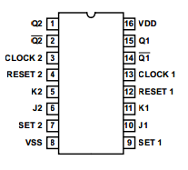
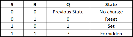
CD4027 is a JK flip flop, master slave which is employed in toggle mode. IC is used to alter the signal by providing control input from one or more input and get output at one or more output terminal. The value of output not merely depends on the present input state but also on what is the present state (also depend on the earlier state). Memory circuit inside the computer mainly used flip flop. There are four input pins in JK flip flop named J and K along with set and reset pin and Q and Q¯ for output. The value of Q and Q¯ are opposite of each other i.e. if the value of Q is higher than the value of Q¯ being low and the output at both the terminals depend on in what way input is configured.The diagram shown below the IC pin configuration. Logic level present at the input terminal J and K along with internal control is used to control the stage of flip flop. At every positive going cycle change occur in the state. Set and reset pin in this is not dependent on clock pulse and when a high signal is given at any of the input terminals sets and reset pin initiated. The circuit described is triggered on the foremost rim of the switch pulse i.e. when the switch is pressed once its output alter. As shown in the circuit that both input terminal J and K are set of high value which implies that at each positive or negative transition the pulse of clock fluctuate between high to low. This condition of the flip flop is called forbidden state and with the help of truth table below explains these conditions can be verified. A small clock pulse will given to the input of IC as soon as you press the switch as a result of it pin 1 output became high. Till the second pulse will receive the output remain high. Load or Led attached with output activates. When the second clock pulse reaches on pin3 IC output turn low and LED or load attached to it become off. This circuit works on pressing the switch but if you wish to break the circuit all you need is to just swap the position of the switch and resistor. Comment * Name * Email * Website
Δ
![]()
![]()
![]()
![]()
![]()

