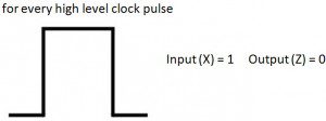
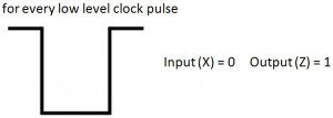
We use not gate functioning in NOR gate and NAND gates.
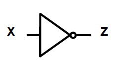
NOT Gate Logic Symbol and Boolean Expression
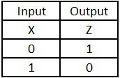
We know the NOT gate is an inverter, which inverts or reverses the input.. So the output is represented by ‘-’ bar symbol of the input. The Boolean expression of the NOT gate is Z =X ̅. Pronounced as “Z is equal to X bar”. The logic symbol of the NOT gate is shown in below figure. If X is the input and Z is the output, then if X = 0, then Z = 1 If X = 1, then Z = 0.
The bubble at the output port represents the inverting operation. That means for high logic signal input, the output of the NOT gate will be LOW, similarly for low logic signal input the output of NOT gate will be HIGH. We can easily understand this by truth table stated below.
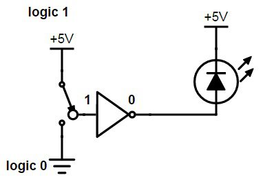
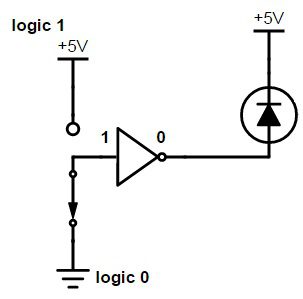
Explanation of Not gate with light switch circuit
The NOT gate can be easily understood by using a LED (light emitted Diode) circuit. This is also called Light switch circuit. In this circuit, NOT gate functions like an electronic switch. When it got high input, the LED connected at the output will be OFF, as the output of NOT gate becomes 0. In the same way, when the logic gate is connected with LOW input, the LED will be ON, as the output becomes 1. The Light switching circuit with NOT gate is shown below.
Here we connect an alterable switch with the NOT gate and the output of NOT gate is connected to a LED. An LED is an electronic device which will ON and off when it receives high voltage and low voltage respectively. When the switch is connected to +5 V, the switch is on position so the LED emits light. When the NOT gate is connected to Ground, the LED will OFF so it doesn’t emit any light. Back to top
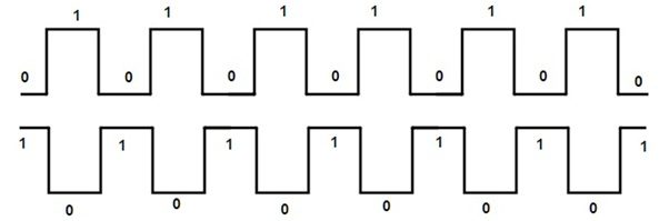
Pulsed Operation
When we apply a pulse signal to the NOT gate, it will ON and OFF for HIGH and LOW levels respectively. This means,
For a sequence of clock pulses, the input and outputs of NOT gate will be If we observe the above diagram, we can observe how the input will invert for every HIGH and LOW pulses of a clock cycle.
Back to top
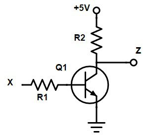
Not Gate using NPN Transistor
We can design a NOT gate by using a NPN transistor as shown in below picture. The Base (B) of the NPN transistor is connected with the input signal X. we connect a supply voltage of +5 V to the emitter (E) and the output Z is collected at the emitter. When the low level voltage 0 V is connected to the input, then the transistor will be OFF. So no current flows through it. This means the supply voltage +5 V will be measured at the output port, which is considered as HIGH state.
Similarly, when the high level voltage +5 V is connected to the input, then the transistor will be ON. So the total supply current will be drawn by transistor. This means the no voltage is measured at the output port, which is considered as LOW state. At this situation the output voltage is measured as +5 V, which will be considered as HIGH logic level. The transistor designed NOT gate is shown below.
Back to top
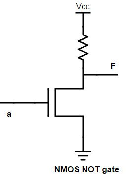
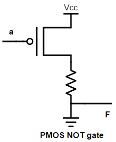
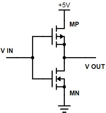
CMOS Transistor as Inverter
CMOS means – complementary Metal oxide semi- conductor.CMOS inverters are widely used and MOSFET inverters find their use in chip design. Another advantage of CMOS inverters is that they have large noise margin in both high and low logic states and have good logic buffer characteristics also. A CMOS inverter has an nMOS and a pMOS transistors, connected at Drain and Gate. The supply voltage VDD is given at the source terminal of pMOS and the source terminal of nMOS transistor is grounded. The input voltage Vin is given at the gate terminals and the output Vout is collected at drain terminals. The key point to remember about the CMOS inverter is that it doesn’t contain any resistors so there is no voltage drop. This makes the CMOS inverter more power efficient. Whenever the input voltage of the CMOS inverter varies between 0 volts and 5 volts the state of PMOS and NMOS also varies.
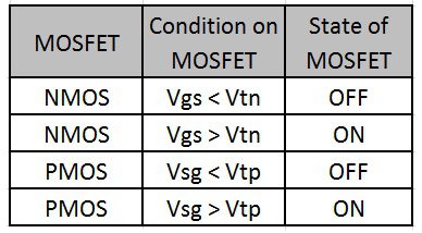
The switch conditions will depend on the Drain, Source and Gate voltages, which are explained as
Back to top
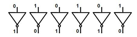
Representation of Active – low input using bubble
The complement operation performed by not gate is represented using a bubble at the input or output of the logic gate. This bubble indicates the Active low input. This logic gates with representation of active low inputs are shown below.
The indication of active low inputs or the bubble at the NOT gate represents that an input will effect the logic gates only when the inputs are low. Back to top
NOT Gate using NAND and NOR Gates
NOT gate can be designed by using NAND or NOR gates also.
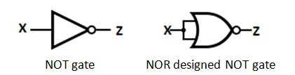
From NOR gate
We know that the NOR gate is the combination of OR gate and NOT gate. So we can design the NOT gate by eliminating the OR part of the NOR gate. The NOT gate design from NOR gate is shown below.
The Boolean expression for the NOR used NOT gate is given as Output (Z) = NOT (A + A)
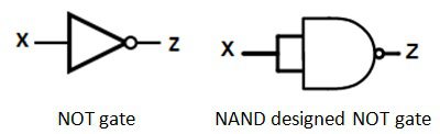
From NAND gate
We know that the NAND gate is the combination of AND gate and NOT gate. So we can design the NOT gate by eliminating the AND part of the NOR gate. The NOT gate design from NAND gate is shown below.
The Boolean expression for the NAND used NOT gate is given as Output (Z) = NOT (A . A) Back to top
Commonly available TTL and CMOS Logic NOT Gate IC’s
74 series ICs
74 LS 04 – hex NOT 74 LS 05 – hex NOT with open collector outputs 74 LS 14 – hex NOT with Schmitt Trigger inputs
4000 series ICs
4000 – Dual 3-input NOR gate + 1 NOT gate 4007 – Dual complementary pair + 1 NOT gate 4572 – Hex gate, quad NOT, single NAND, single NOR 40106 – Hex inverting Schmitt trigger-(NOT gates)
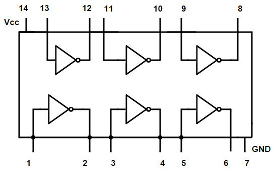
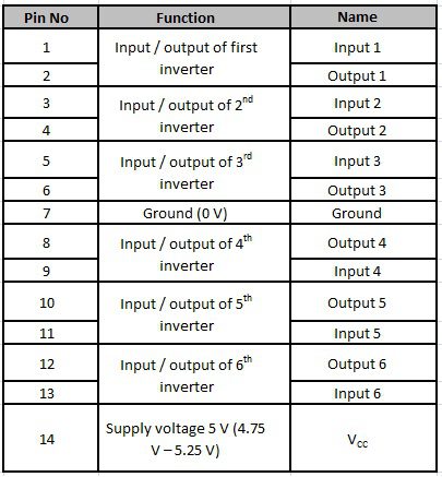
7404 Hex Inverter IC
IC 74LS04 is used as NOT gate. Its IC diagram and pin description is given below
Pin description
Back to top
Not Gate Applications
NOT gates produce reverse output of the input, so they are also called “Inverters”. The CMOS inverters are generally used in designing of oscillators. They are used mostly, because of their low power consumption. Another advantage of CMOS inverter is that they can be easily interfaced than other logic devices. The above circuit is designed in a ring format to produce oscillations like square wave oscillator. The frequency is given by F =1/2ntp . Where n is the number of inverters used to construct the oscillator Tp is the propagation delay of each gate. Back to top Comment * Name * Email * Website
Δ
![]()
![]()
![]()
![]()
![]()

