Introduction to ATtiny85 Microcontroller
The ATtiny85 is a tiny, 8-pin Microcontroller from Atmel (now part of Microchip Technology). It is a low-power 8-bit AVR microcontroller based on modified Harvard RISC Architecture. It has 120 powerful instructions, most of which execute in a single clock cycle. Hence, you can expect an impressive throughput of 1MIPS per MHz with very low power consumption. For example, if you have a 16MHz clock frequency for ATtiny85, then it is possible to get 16MIPS throughput. ATtiny85 has 8KB of ISP (In-System Programmable) Flash Memory, 512B of EEPROM and 512B of SRAM. These numbers might not seem impressive but considering the small size, low-power and its throughput, we can manage with these memory configurations for small to medium applications. Using the on-chip flash memory, you can program the microcontroller using SPI ISP or through USB with additional bootloader code. Note that, depending on the type of boot code, it might take up to 2KB of the flash memory. Leaving you with only 6KB program memory. There are several other important features and specification of ATtiny85, which we will see in the next section. Digistump developed the Digispark ATtiny85, a tiny development board based on the ATtiny85 Microcontroller. It is very small, smaller than a regular flash drive. The reason we are comparing it with a flash drive is because the Digispark ATtiny85 development board has an on-board USB connector, right on the PCB itself. You can just plug it into a computer’s USB port to program or power it on.
Important Specifications of ATtiny85
In in the introduction section, we saw just a couple of important features and specifications of ATtiny85 Microcontroller. Here are some more specifications.
Low Power 8-Bit Microcontroller Modified Harvard RISC Architecture 8KB Flash Memory 512B EEPROM 512B SRAM 8-bit Timer/Counter with 2 PWM Channels 8-bit High Speed Timer/Counter USI (Universal Serial Interface) Four 10-bit ADC Channels Watchdog Timer and Analog Comparator On-chip Debug System (debugWIRE) ISP (In-System Programming) via SPI Support for external and internal interrupts Power-ON Reset, Internal Oscillator, Brown-out Detection Operating Voltages: 1.8V – 5.5V for ATtiny85V and 2.7V – 5.5V for ATtiny85 Speed Grade for ATtiny85V: 0 – 4MHz at 1.8 – 5.5V, 0 – 10MHz at 2.7 – 5.5V Speed Grade for ATtiny85: 0 – 10MHz at 2.7 – 5.5V, 0 – 20MHz at 4.5 – 5.5V Active Mode Power Consumption: 300µA at 1MHz and 1.8V Power Down Mode Power Consumption: 0.1µA at 1.8V
Please refer to the datasheet of ATtiny85 Microcontroller for a more detailed and complete set of features, specifications, Pinout, pin functions, registers and many more.
ATtiny85 Pinout and IC Packages
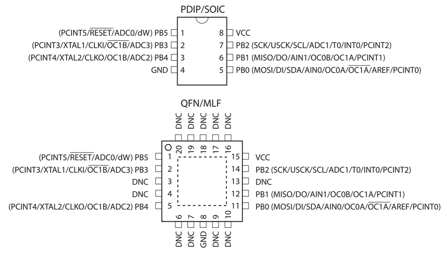
The pinout of any microcontroller is dependent on it packaging styles. So, in order to understand the ATtiny85 Pinout, we have to first take a look at all the available IC Packages of ATtiny85 Microcontroller. Like any modern microcontroller, the ATtiny85 is also available in multiple IC packages. Since it is a tiny device, it is available in 8-pin PDIP, 8-pin SOIC and 20-pad QFN packages. The pinout of both the 8-pin packages i.e., 8-pin PDIP and 8-pin SOIC is the same. But an interesting point about the 20-pad QFN package is that even though it has 20-pads, 12 of its pads are DNC (Do Not Connect). So, this leaves us with the essential 8 functional pads. In the following image, we present to you the IC Packages and also the ATtiny85 Pinout for those packages.
From the above image, it is clear that each pin of the ATtiny85 Microcontroller is heavily multiplexed with some pins having up to 9 different functionalities (of which, you can use only one).
Pin Description of ATtiny85 Microcontroller
Now that we have seen the ATtiny85 Pinout for all the IC Packages, let us now dive into the pins of the Microcontroller along with their functions. We put together a comprehensive table with all the pins, their alternative functions and also the pin description. Please note that this pin description is just a brief overview of the functionality that a pin can offer. For in-depth understanding of the pin functions and also how to select a proper function through the multiplexer, you have to go through the datasheet of ATtiny85. ADC Input Channel 0, Pin Change Interrupt 5 External Clock IN, ADC Input Channel 3, Complementary Timer/Counter 1 Compare Match B OUT, Pin Change Interrupt 3 ADC Input Channel 2, Timer/Counter 1 Compare Match B OUT, Pin Change Interrupt 4 Timer/Counter 0 Compare Match A OUT, Complementary Timer/Counter 1 Compare Match A OUT, USI Data IN (3-Wire Mode), USI Data IN (2-Wire Mode – I2C), External Analog Reference Pin Change Interrupt 0 Analog Comparator Negative IN, Timer/Counter 0 Compare Match B OUT, Timer/Counter 1 Compare Match A OUT, USI Data OUT (3-Wire Mode), Pin Change Interrupt 1 Timer/Counter 0 Clock Source, USI Clock (3-Wire Mode), USI Clock (2-Wire Mode – I2C), External Interrupt 0 IN, Pin Change Interrupt 2
Conclusion
This was a brief introduction to the ATtiny85 Microcontroller, a low-cost, low-power 8-pin microcontroller from Atmel (Microchip Technology). We saw the important features and specifications of the ATtiny85 Microcontroller. Then, we looked at the different IC Packages and also the ATtiny85 Pinout for those packages. And finally, we saw the pin description for all the pins along with a list of their alternative functions. Comment * Name * Email * Website
Δ


![]()